PCE stimulates design opportunities
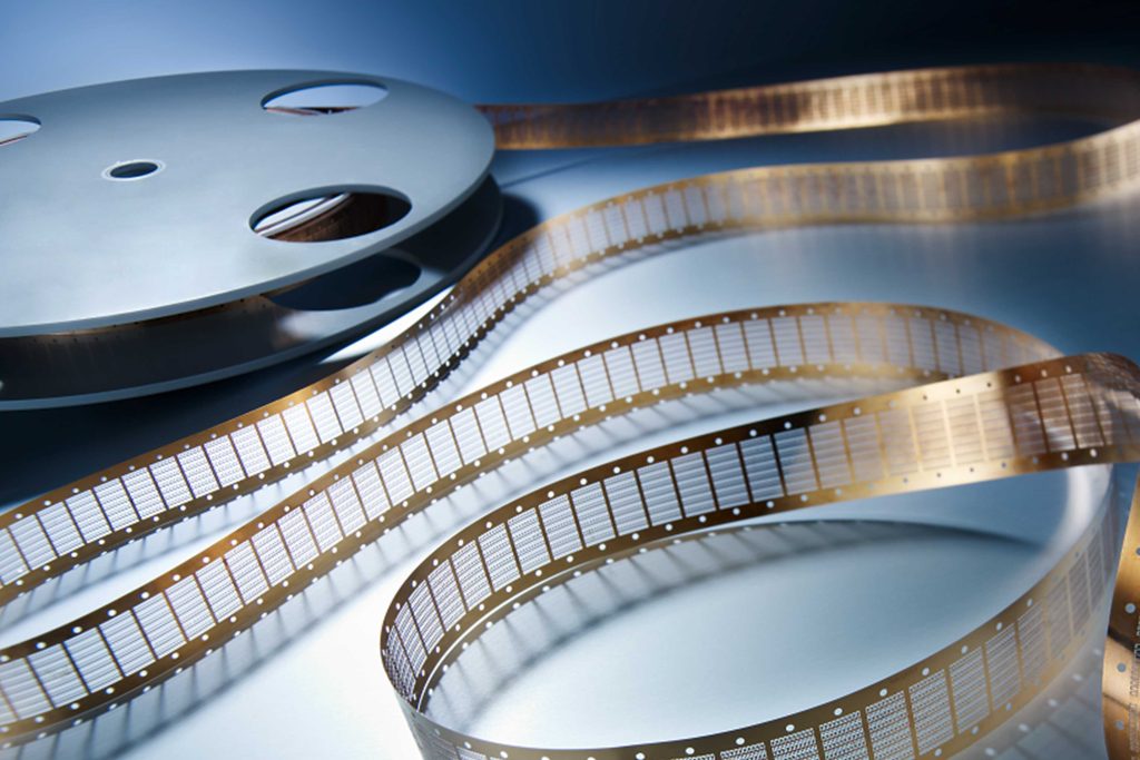
It is well-known today that photo-chemical etching (PCE) is a precise and cost-efficient way to fabricate complex parts with intricate geometries, tight tolerances, and highly repeatable results for large production runs. However, what is less well known is how this technology is evolving, and also what this evolution means for the stimulation of design freedom.
micrometal GmbH is at the forefront of PCE development, and as such is helping industry to innovate ever more complex and intricate parts and components.
Jochen Kern, Head of Sales & Marketing at micrometal GmbH says, “As a spur to design freedom, the precision and repeatability of PCE is an important starting point. At micrometal, we have taken what was already a precision process and refined it to make the world’s most precise PCE process. Our etching process is very different from conventional PCE processes. We use a special liquid resist system to obtain ultra-thin photoresist layers enabling a higher degree of precision in the chemical etching process. It allows us to achieve extremely small feature sizes and single digit micron tolerances repeatably. Traditional PCE uses relatively thick dry film resist which compromises ultimate part precision and the tolerances that are available. In production, we also use glass photomask tools printed at 100,000 dpi, providing superior reproduction and resolution than film photo-tooling used in conventional chemical etching processes.”
The use of digital tooling is one of the key characteristics of PCE that lifts the lid for design engineers. No need for tooling investment and short tool lead times makes design modification easy, and this flexibility means design engineers can think outside the box, and test new design conceptions that would be too costly and time-consuming using traditional manufacturing processes.
Adding to this agility, micrometal’s unique PCE process is able to achieve dimensional tolerances as a low as +/-0.005mm, small feature sizes of 25 microns, a minimum hole diameter 80% of the material thickness, and single digit micron tolerances repeatably. Compare this with traditional chemical etching which is only able to achieve a smallest feature size of 100 microns, and the smallest hole diameter is a factor of 1-2 when compared to material thickness. and it is easy to see how micrometal’s PCE process opens up numerous hitherto impossible design opportunities.
Kern continues, “With ultra-precision comes almost limitless geometric complexity when using micrometal’s PCE process. Complexity does not add time or cost as would be the case with traditional manufacturing processes, so you can design and prototype a number of versions of an impossibly complicated part in a matter of days. In addition, the process itself has some unique attributes — such as etch cusp — that make the inclusion of otherwise challenging product features such as sharp edges and conical openings simple. By understanding the physical properties of the material being etched and how the process works, designers can create components that are not only more efficient in their end use applications, but also where it is advantageous more aesthetically pleasing. This is best done working in close collaboration with the photo-etching specialist that can help design for PCE (DfPCE).”
PCE has an important role to play in stimulating design freedom. It offers a number of advantages over traditional manufacturing processes such as lower costs, greater precision and accuracy, faster lead times, and the ability to create complex shapes with minimal effort. By choosing micrometal’s PCE for your next project you can unlock a world of possibilities that would normally be confined by conventional technology and even by alternative legacy PCE.